Wiring the Alarm Clock

This guide provides details for learners to wire, program and configure their first @ShrimpingIt Arduino-compatible digital clock project. For general orientation, see the Alarm Clock project page. The completed build should replicate the image shown on the left.

For convenience, pre-bagged kits are available to order from @ShrimpingIt online. If you do not wish to buy from us, information is provided for you to source commodity parts direct from electronics wholesalers.

Getting started

Before embarking on the Alarm Clock, you should have successfully completed the Blink build. This build uses the Blink circuit as its starting point.

Remove surplus parts

You can remove the Blink LED and resistor as these are not used in the circuit, and it will be easier to wire the circuit with them out of the way.

Decoupling Capacitor

We are planning to deploy this circuit in the real world for a long time. We would like it to be stable to momentary changes to its power supply, (e.g. when a motor or a large number of LEDs suddenly draw a lot of energy from the same source).

If the voltage drops too low, the Shrimp's ATMEGA328P-PU microcontroller will reset itself. Adding a decoupling capacitor provides a very short-term reservoir, decoupling the microcontroller from temporary dips in supply voltage.

The S.I. unit of capacitance is the Farad, indicating how much charge can be stored at a given voltage. Capacitors are labelled with the number of picoFarads capacitance, with the last figure indicating the number of zeroes to tack onto the number. We will be using a small ceramic capacitor labelled 104. This means it's 10(0000) picoFarads. There are 1000 picoFarads in a nanoFarad, so that's equivalent to 100 nanoFarads. Ceramic capacitors are symmetrical and can be inserted either way around.

Insert a capacitor labelled 104 between the 5V and GND Power rows D9 and D10

Right Hand Power Rails

The power rails of your 400 point breadboard are four very long contacts which run in pairs down each side of the breadboard. They can help provide a power connection close to any component in the circuit.

They are called power rails because two crucial connections are needed for components to get power. In this circuit the two power connections needed are 5V (VSS or VCC) and 0V (Ground or GND). We will only be attaching the rails on the right of our breadboard.

The columns often have a red or blue line running alongside them. We will follow the convention that the red column will be used for the +ive voltage supply of the circuit (in our case +5V) and the blue line offers a connection to ground (0V).

Although the vertical columns of holes each side of the breadboard are presented in groups of five, each column actually contains a single contact. Any wire inserted in any group of five holes is connected to every other wire inserted in the same column, even if it's inserted in a different group. Note this is completely different to breadboard rows, where every group of five is isolated from every other.

Connect a Green wire between J9 and any hole in the right-hand Blue column (connecting the Ground Rail)
Connect a Red wire between J11 and any hole in the right-hand Red column (connecting the +5V rail)

DS1307 Real Time Clock

The DS1307 Real Time Clock chip will be used to keep accurate time in our circuit. It looks a bit like a dead bug.

The chip must straddle the central spine of the breadboard. Each leg has a different number, name and function and should be cleanly inserted into a separate breadboard row with a minimum of bending. We can then wire components to a leg by inserting them in the same row.

The chip must be placed the correct way up. You may notice a half-moon shape punched in one end of the chip. A small circle is sometimes punched in one corner (indicating which is Pin number 1). The half-moon should be at the top of the circuit and any circle should be positioned toward the top left (the DS1307 has the same orientation as the Shrimp's ATMEGA chip).

It is called a chip or an Integrated Circuit (IC) because it contains a doped silicon wafer or 'chip' from which tiny shapes are cut, constructing the electronic components which make the clock circuit. The circuit inside is connected to the two rows of four legs.

Pins are numbered sequentially from Pin 1 (top-left, where a circle is punched in the plastic housing) anticlockwise around the chip until pin 8. The wiring for each pin is described in the following list. If you want, you can ignore this list and simply follow the step-by-step instructions which follow.

  • Pins 1&2 - two sides of a crystal which oscillates at 32.768Hz
  • Pin 3 - the +ive side of 3V coin battery attached as a backup to keep time
  • Pin 4 - ground rail 0V (GND)
  • Pin 5 - to ATMEGA SCL pin (is set to +5V when SDA has a one or zero value ready)
  • Pin 6 - to ATMEGA SDA pin (is set to +5V to represent a one, or 0V to represent a zero when sending binary data - used with Pin 5)
  • Pin 7 - Sends an accurate heartbeat, e.g. an attached LED flashes once a second
  • Pin 8 - Connected to the supply rail 5V (VCC)

Place the chip straddling the gap in the centre of the breadboard, with pin 1 (anticlockwise from the half moon) in e20, and the opposite corner (known as pin 5) in f23

DS1307 Power

The DS1307 chip needs power for it to run. Now the right hand power rails are connected, we can easily get a +5V or 0V connection for any component in our circuit.

Connect a Red wire from j20 to any hole in the right-hand Red column (connecting to +5V)
Connect a Green wire from d23 to any hole in the right-hand Blue column (connecting to 0V)

Wire ATMEGA328 to DS1307

The Shrimp's microcontroller and the RTC chip communicate using a protocol known as "Inter-Integrated Circuit" or I2C. This is also known as the 'Two Wire Interface" as bidirectional communication between multiple ICs can be sent along just two wires, one wire which pulses on when binary data should be read, and another wire which sends binary data (as ons and offs) timed to the pulses.

Connect the Purple SCL wire from i3 to h22, connecting the ATMEGA's SCL pin to the DS1307 SCL pin
Connect the Yellow SDA wire from i4 to i23, connecting the ATMEGA's SDA pin to the DS1307 SDA pin

I2C Pull-up Resistors

Chips communicating over I2C use an 'active low' to communicate. The circuit should be wired to maintain the SCL and SDA lines 'pulled up' at 5V (but not very strongly - using resistors to limit the influence of the 5V signal).

When an IC wants to signal, it drags down the voltage of the SCL or SDA lines to 0V with a much more powerful signal. Other ICs attached to the same wires can detect this change. Both SCL and SDA wires should be attached to 5V through a fairly large resistor.

Resistors are labelled with colored stripes instead of numbers, but using the same system as the '104' capacitor earlier. Decoding the colors Brown=1, Black=0, Orange=3 gives us the number 103. That means the resistance in Ohms starts ‘10’ and continues with a further 3 zeroes – 10(000) Ohms or 10 kiloOhms.

** Attach a 10kiloOhm pull-up resistor between j3 and any hole in the right-hand Red column, connecting SCL to +5V
Attach a 10kiloOhm pull-up resistor between j4 and any hole in the right-hand Red column, connecting SDA to +5V
**

Crystal for DS1307

The crystal is a small silver cylinder with two wires coming out of one end, probably marked "32.768kHz".

The DS1307 Real Time Clock chip needs a special piece of electrically oscillating material, known as a crystal to use as a pendulum for the clock. This material is coupled to a circuit inside the DS1307 which causes the material to resonate, generating high and low voltages, just like a pendulum swinging backwards and forwards driven by clockwork.

Hz is a measure of how many times a second something happens, and k means kilo, or 1000, so we would expect this crystal to oscillate 32.768 thousand times every second.

Backup Battery Holder

The holder is a Black plastic circular module with two pins coming from the base. If the coin cell is inside the battery holder, remove it. We'll add it back later.

The holder is designed to hold either a CR2032 or LIR2032 (rechargeable) battery rated at around 3V. We've not added a recharging circuit to keep things simple, so we can use the cheaper CR2032 3V disposable battery. If wired correctly, it is still expected to last significantly more than a year as a backup for this clock.

We need to insert the holder with the square bracket towards the top of the breadboard. As you insert the holder, look from the side, and note where the positive pin (at the square end) passes into the breadboard; it should enter into the row parallel to pin 3 - the battery backup pin on the DS1307. Note where the negative pin (at the round end) passes into the breadboard; it should enter at a30 which is not yet connected to anything else.

Finally the negative pin of the battery holder needs to be connected to the common ground of the circuit. As any ground connection will do, we connect from row 30 back to the nearby ground pin of the DS1307 for convenience.

Add the backup battery holder, with the +3V positive pin (the square end) inserted at a22, and the 0V ground pin (the round end) inserted at a30, connecting the +3V pin to pin 3 of the DS1307
Add a green wire from e30 to c23, completing the battery backup circuit

Piezo Transducer

Unless we add a display, (as detailed in the LED Clock Addon ) the only output of this clock will be a piezo beeper, which can play Nokia Ringtone (RTTTL) tunes according to scheduled alarms you program in.

Piezo is short for Piezoelectric transducer. It uses a piezoelectric effect where applying a voltage generates flexing within a ceramic material. The effect is reversible, as flexing it also generates a voltage. For this reason the component is called called a transducer as it can be used for output OR for input.

The piezos we are using have no orientation and can be inserted either way around.

Insert the Piezo so that one of its pins goes into row 26, and the other goes into row 28, keeping it as far to the left as possible

Piezo Ground wire

We want the Piezo to experience a voltage across the material, so it will need to have a connection to 0V (ground) on one side, then we can control the voltage of the other side. We will connect the ground rail with a 'current-limiting' resistor. Using a resistor instead of a wire reduces the amount of power sent to the Piezo, making the circuit more stable.

Attach a 100 Ohm resistor wire between the right-hand -ive (Blue) power rail, and hole j28

Piezo Control wire

We will be varying Arduino pin 6 on the ATMEGA chip between 0V and 5V using its special PWM capabilities to cause the Piezo to flex back and forth, making sound.

Attach a wire between d14 and j26, connecting the Piezo to the pin we'll use to generate audible waves; Arduino pin 6

Insert Coin Battery

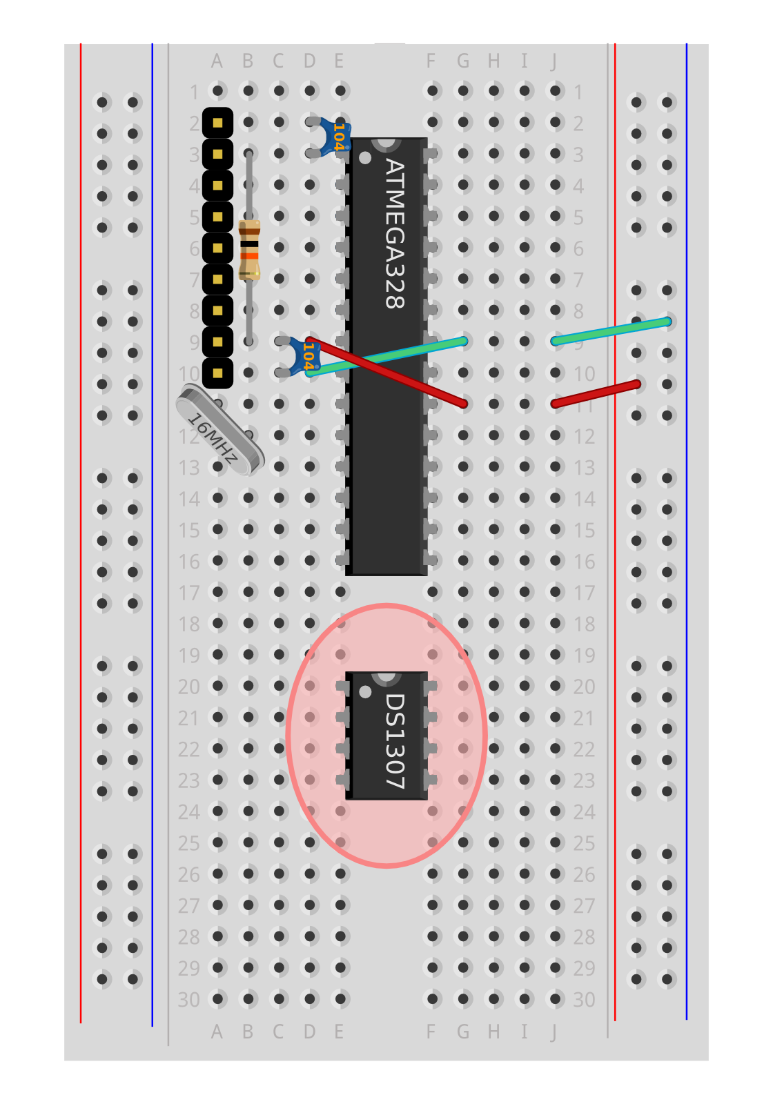
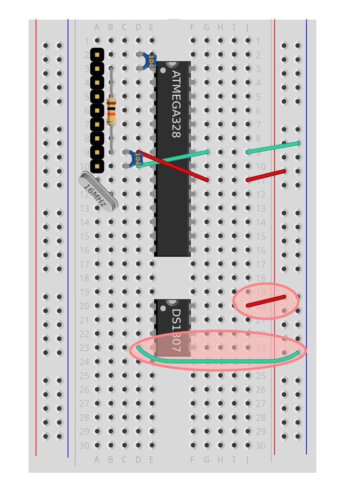
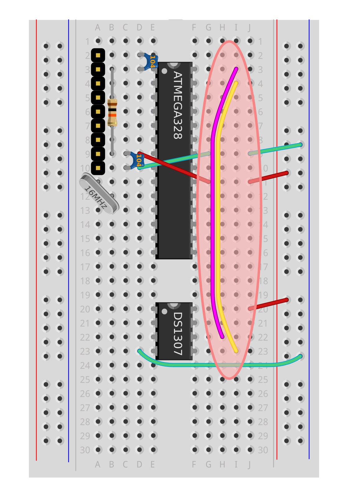
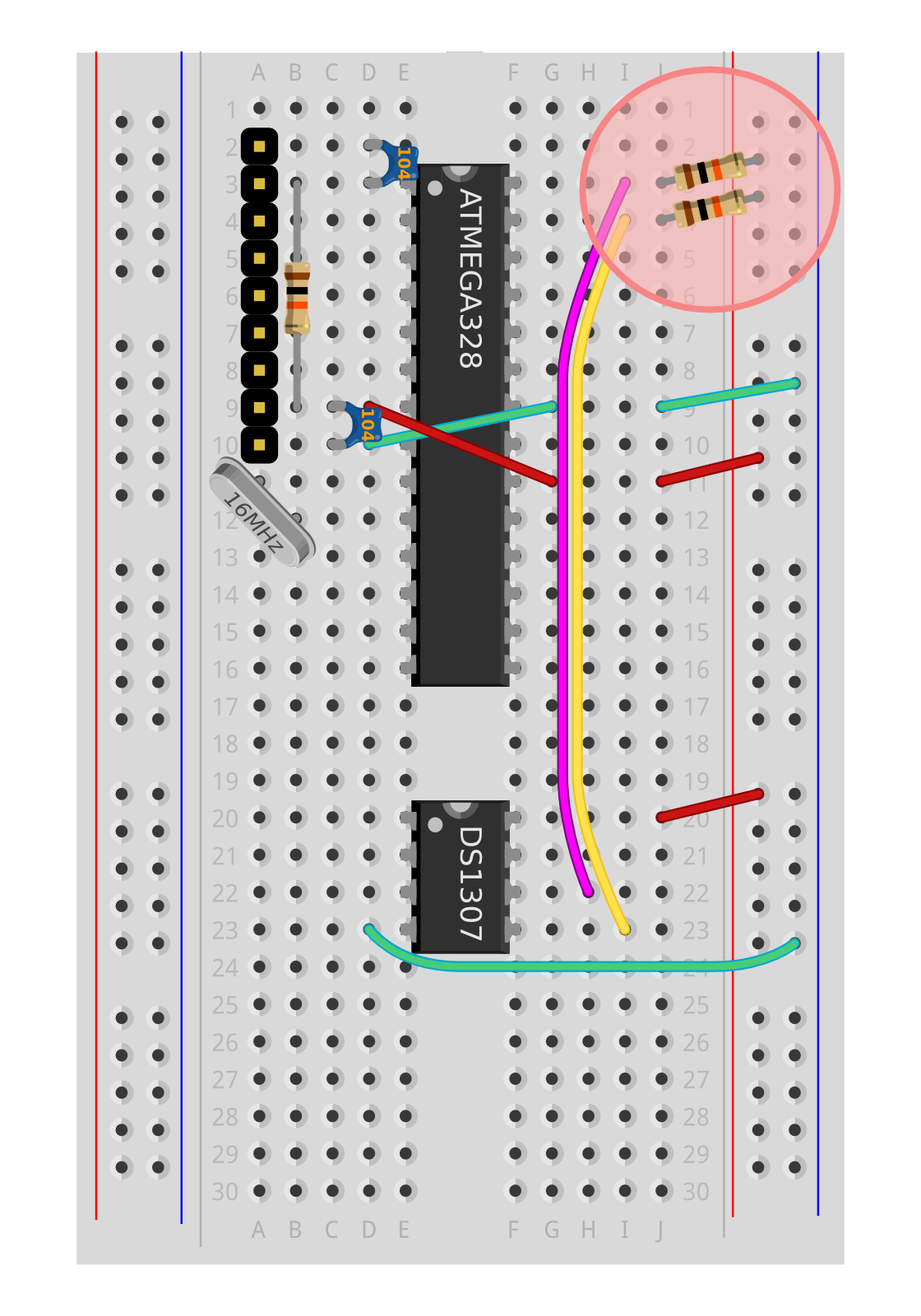
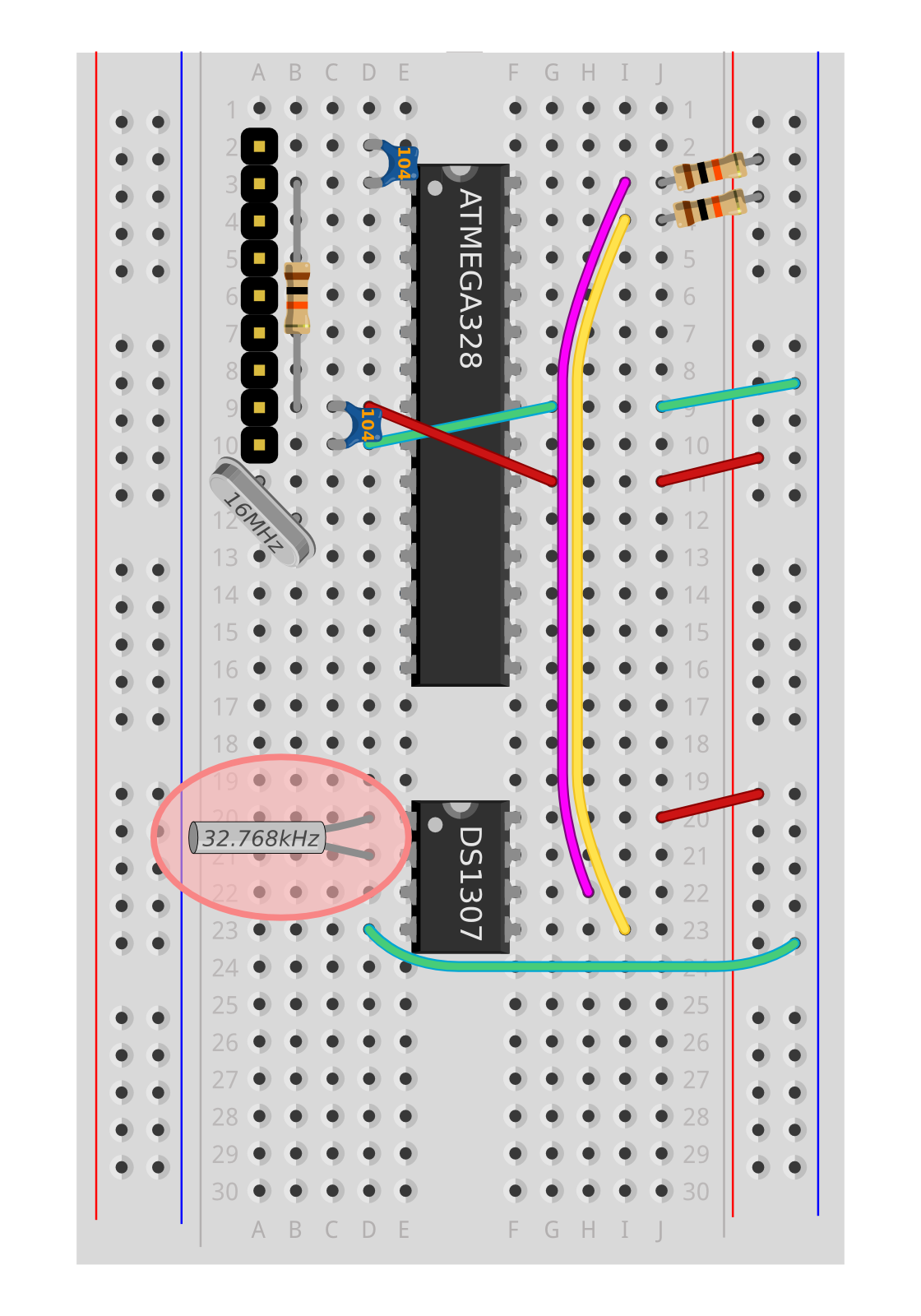
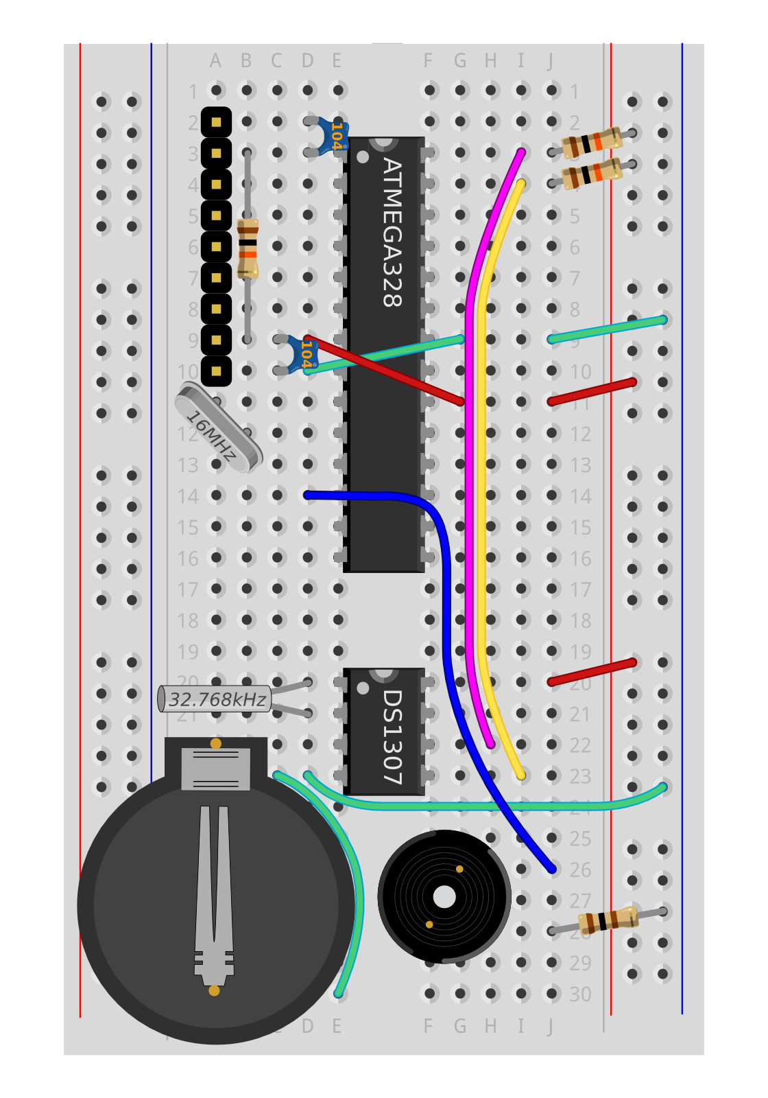
After double-checking your layout matches the final diagram above, you can insert the coin battery. Once you have set the time, this will help your clock keep time even when the USB or main battery pack is removed.

Note, if you attach nothing to the DS1307 Battery pin, then the clock will not work at all. If you don't have a reliable coin battery, and want to test your clock programming by powering the DS1307 from the 5V supply, you need to attach DS1307 Pin 3 (the positive side of the coin battery) to 0V (ground). This tells the DS1307 to use the main power supply instead of the coin battery. Note, if a coin battery is attached at the time, this will short the battery!

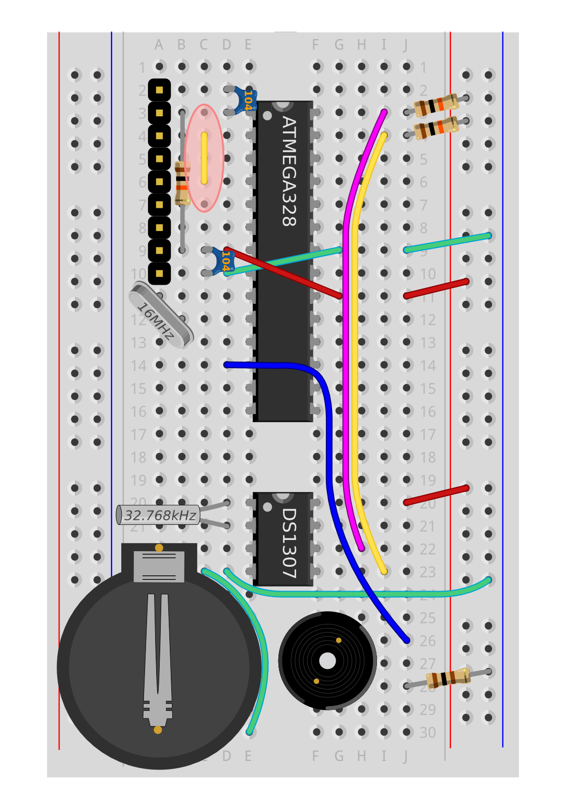
A workaround to ground DS1307 Pin 3, which avoids battery shorting, is to remove any battery, and balance a small metal disc or coin in the place of the battery, being sure that it touches both terminals. This effectively connects Pin 3 to Ground. A piece of card cut to size and wrapped in aluminium foil is a good option.

For any clock behaviours to work (such as playing chimes) you must attach a reliable power supply of 3.6V to 5V, which you can get by plugging into USB or by wiring in a 3xAAA battery pack.

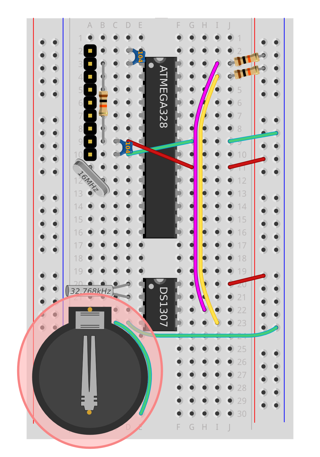
Check the circuit, then add the coin battery, with the plus-sign upwards, placing the edge under the two lugs, and pressing until the silver catch clicks.

Upload Code

Now the clock subcircuit is complete, we can set and read back the time from the clock. Verifying this simple behaviour is a useful test, before we add extra hardware for a specific time-based project, or extra logic for controlling different chimes.

In later steps we add a special subcircuit allowing the Clock to be woken from a LowPower state by sending over Serial, and add some buttons which can be used for controlling the Alarm. However the fundamental hardware is all in place, and we can already start to program our clock.

Visit the programs page to configure your programming environment and program the circuit with the Clock01HardcodeTime or Clock02SetTime programs.

Wire for Serial Wake

This wire allows us to monitor activity on the Serial data in wire using Arduino pin 2, a pin which is capable of waking the chip from a low-power sleep mode. This is demonstrated by the Alarm04LowPower sketch.

Interactive Buttons

Buttons can be added to allow you to control your clock in different ways, for example as a Snooze button, or to advance or retard the time or alarm time.

Button Ground wires

Once the Ground wires are attached, the buttons can be configured in software by setting Arduino Pin 7 and Pin 8 pinMode() to be INPUTPULLUP, then they can be detected by using digitalRead.